

At 8.46" x 8.46", the chip is 56 times larger than the biggest GPU (graphics processing unit), a Nvidia chip that’s Lilliputian both in size and capacity alongside the trillion transistors etched into the Cerebras. Nearly 200 engineers at Cerebras have spent the last three years quietly developing the wafer-scale engine for AI applications.
The specs for the Cerebras Wafer-Scale Engine are astounding. Cut from a 300mm (12") wafer, elements of which are programmable and able to serve various purposes, the chip has:
- 1.2 trillion transistors,
- 400,000 AI programmable cores,
- 18 GB of super-fast, on-board memory (SRAM),
- 9 Petabytes/s memory bandwidth, and
- Software compatibility with standard AI frameworks such as Google’s TensorFlow and Py Torch.
According to the cofounders, hardware architect Sean Lie and CEO Andrew Feldman, the chip is designed to serve the demands of AI with “vastly more deep learning compute.” There are 400,000 SLA (sparse linear algebra) cores that the developers explain are “flexible, programmable, and optimized for the computations that underpin most neural networks. Programmability ensures the cores can run all algorithms in the constantly changing machine learning field.” Essentially, the dinner plate-sized chip is a supercomputer for AI applications.
WHAT HAPPENED TO MICROCHIPS?
When you think of computer chips, you probably think of something that might fit, or even get lost, in the palm of your hand. That’s probably due to the definition of the word. Techopedia’s definition reads: “In electronics, a chip is comprised of semiconductor material that is cut from a large wafer of material that is only a few millimeters on one side. On this chip, a transistor or integrated circuit may be etched but only occupy one-thousandth of an inch of the chip’s surface.” Hence, we picture micro elements electronically scribed onto a very small piece of silicon. And the definition is applied broadly, because “The terms chip, microchip, integrated circuit (IC), and silicon chip are synonymous.”
In fact, the universal expectation for those tracking Moore’s Law is that new chips will become more powerful as they shrink to ever smaller sizes. Conventional manufacture of chips involves a relatively large wafer of silicon that receives the electronic components many times over, and at the end, the individual chips are cut free and tested, and those that work get sold. It’s planned this way because many fail, and this method has proven to be less wasteful.
But now, the incredible shrinking chip has exploded. Cerebras has found a way to assure functioning chips across the surface of the entire wafer, and communication between the chips is done right at this stage of the manufacture. You don’t have to cut them out and wire them to other chips later.
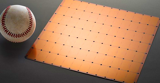
An idea of relative size Images courtesy Cerebras
GPUS TODAY—AI NETS TOMORROW
Cerebras’s super-size chip isn’t the first attempt at this kind of architecture. In 1980, chip designer Gene Amdahl raised $230 million for his Trilogy project. The unsuccessful attempt to build a chip the size of a complete wafer lasted for five years.
Since then, Google has built the tensor processing unit (TPU), an AI integrated circuit, specifically designed for neural network machine learning, which is used in a variety of AI applications like Google Assistant and Google Translate. And other chip makers are investing heavily in research in pursuit of powerful, integrated chips for AI processing.
Rakesh Kumar, a professor at the University of Illinois and researcher into large chips for AI, is cited in The New York Times, “It is not that people have not been able to build this kind of chip. The problem is that they have not been able to build one that is commercially feasible.”
The growing interest in the field is due to the commensurate interest in AI. The kind of chip commonly used today for analyzing the data are graphics processing units (GPUs) like the one standing alongside the WSE in the photo at the beginning of this article.
Newer AI systems use neural networks, computer systems patterned after the brain and human nervous system. These ANNs, artificial neural networks, or neural nets for short, use numerous processors operating in parallel and arranged in tiers. The many chips have to be connected together, and that slows them down. If you could keep all the data on a large integrated chip, “a massive chip for massive processing,” speeds would increase.
Karl Freund, senior analyst for deep learning and high-performance computing at Moor Insights & Strategy, writes, “Basically, Cerebras designed a wafer of 84 interconnected chips that act as one device for compute and memory, interconnected by a super-fast, on-die fabric. If Cerebras is right, AI might just be the start of wafer-scale integration; applications increasingly demand better performance than available from CPUs. I imagine that Cerebras’s wafer-scale approach could completely transform High Performance Computing, if it turns its attention to floating-point cores once it finishes with its first AI-focused implementation.”
THE ROLLOUT
Cerebras has published its own specifications for the WSE chip, but these claims need to be tested and verified by others. The founders say they’re working with several major customers, and they plan to ship production servers using the WSE by mid-2020. Freund concludes in his post, “If Cerebras delivers a solution that is 1,000 times faster than the competition, at a reasonable price and power envelope, I believe the ecosystem will beat a path to its doors.” For now, there are still quite a number of “ifs” to be resolved.

